

Double-layer circuit PCB board copy method:
1. Scan the upper and lower layers of the double-layer circuit board and save two BMP pictures.
2. Open the PCB copy software Quickpcb2005, click "File" "Open Bottom Image", and open a scanned picture. Use PAGEUP to zoom in on the screen, see the pad, press PP to place a pad, see the line and follow the PT line...just like a child drawing, draw it in this software, click "save" to generate a B2P file.
3. Then click "File" and "Open Base Image" to open another layer of scanned color image;
4. Click "File" and "Open" again, and open the B2P file saved earlier. We see that the board copied from the PCB just now is stacked on top of this picture-the same PCB board, the holes are in the same position, but The line connection is different. So we press "Options"-"Layer Settings", turn off the top-level line and silk screen display here, leaving only multi-layer vias.
5. The vias on the top layer are in the same position as the vias on the bottom picture. Now we can trace the lines on the bottom layer as we did in childhood. Click "Save" again-the B2P file now has two layers of information on the top and bottom layers.
6. Click "File" and "Export as PCB File" to get a PCB file with two layers of data. You can change the board or output the schematic diagram or send it directly to the PCB plate factory for production.
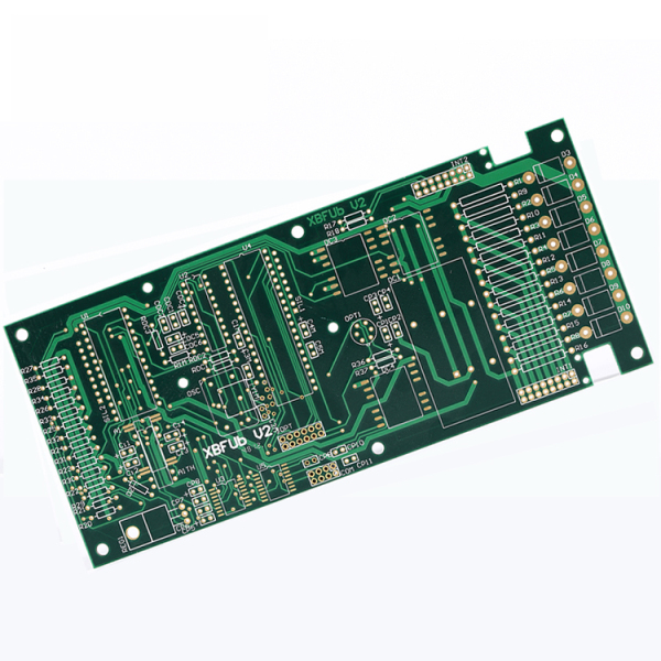
In fact, the copying of the four-layer board is the repeated copying of two double-sided boards, and the six-layer copying is the repeated copying of three double-sided boards... The reason why the copying of a multi-layer circuit board is daunting is because we cannot see the internal wiring. A precision multilayer board, how do we see its inner universe?-Layering.
There are many methods of layering, such as potion corrosion, knife peeling, etc., but it is easy to separate the layers and lose data. Experience tells us that sandpaper polishing is the most accurate.
When we finish copying the top and bottom layers of the circuit board copy board of the multi-layer PCB copy board, we usually use sandpaper to polish the surface layer to show the inner layer; sandpaper is the ordinary sandpaper sold in hardware stores, and the PCB is generally tiled. Press and hold the sandpaper, and rub evenly on the PCB (if the board is small, you can also spread the sandpaper, use one finger to hold the PCB and rub on the sandpaper). The main point is to pave it flat so that it can be ground evenly.
The silk screen and green oil are generally wiped off, and the copper wire and copper skin should be wiped several times. Generally speaking, the Bluetooth board can be wiped in a few minutes, and the memory stick will take about ten minutes; of course, if you have more energy, it will take less time; if you have less energy, it will take more time.
Grinding board is currently the most common solution used for layering, and it is also the most economical. We can find a discarded PCB and try it. In fact, there is no technical difficulty in grinding the board, but it is a bit boring, and it takes a little effort.
Multi-layer circuit board PCB copy board can be regarded as composed of several double-layer circuit board PCB copy boards. As long as the foundation is laid on the double-layer circuit board PCB copy board, the multi-layer circuit board copy board is layered. It can alleviate a lot of troubles of multi-layer PCB copy board.
The above is how to imitate the PCB of the multi-layer circuit board? The introduction of the high-precision multi-layer PCB copy method, I hope it can help everyone and want to know more PCB circuit board information, please follow us.